A while ago I got a ST Nucleo-H753ZI evaluation board because I wanted to try out Hubris, Oxide's embedded operating system. After getting the basic demo app with the blinking lights running I set it aside for a lack of an idea what to do with it. A few weeks ago I was looking through old Raspberry Pi accessories on the hunt for a project. What stuck out to me wasn't any of the Raspberry Pi stuff, but the old 4 by 3 VGA monitor I had standing around. Could I just wire those pins in the VGA cable up to the GPIOs and produce a signal? As it turns out, yes you can just do that.


Getting Rid of the Sys Task
In the beginning I thought I was gonna be changing the GPIO pins from normal code, so switching them
on and off at very high speeds.
In hubris there's a stm32xx-sys task that normally controls the GPIO pins and also handles
enabling clock to the different components through the Reset and Clock Control (RCC) block.
So normally if you want to set a GPIO pin you'd send a message to the sys task and it would do
that for you.
I was worried that the overhead of the context switching was gonna be a problem there.
So I decided to get rid of the sys task and do it all in my task.
The Plan
My first plan was to get the screen to just display a single color. I thought that it would be enough to get the vsync and hsync signals right and then just have the green pin high all the time to get a green picture.
Mapping the Registers
The peripherals of our chip are all controlled with registers. Those are memory mapped and to certain addresses. There is a gigantic 3000 page reference manual that describes all those registers. It's all very overwhelming. Luckily there's a Peripheral Access Crate (PAC) that defines an API for reading and writing those registers.
Since we're running under memory protection we need to first make sure we can actually write to those registers.
In Hubris that sort of thing happens in an app.toml where all the tasks for an app are defined.
[tasks.vga]
name = "drv-vga"
priority = 1
uses = ["rcc", "gpios", "tim3"]
start = true
In this case the tim3 memory region wasn't a thing the Hubris build system knew about yet.
The regions you can use there are defined in a chip.toml for the specific chip you have.
In our case that's chips/stm32h7/chip.toml.
[tim3]
address = 0x40000400
size = 0x400
You get those values from a fun table called "Register boundary addresses" from the manual.
Blinking an LED with a Timer / PWM
The timers on this chip have a Pulse-Width-Modulation (PWM) feature which we should be able to use to generate the VGA sync signals. But the first step was to get a light blinking using PWM. The basic Hubris demo app does have a blinking LED, but that's not using PWM. Instead it uses the timer feature of the kernel, which makes a lot of sense for a Hubris demo, but we want to involve the CPU as minimally as possible for generating the signal.
My initial plan was to measure the PWM with my multimeter to see it working. I chose PB0 for this from the pinout table in the user manual of the board (which is different from the reference manual of the chip). PB0 is hooked up to timer 3, channel 3 (TIM3_CH3). Looking at the "Solder bridges and jumpers" section I found out that that's also connected to an LED on the board by default, so I chose to just test it that way.
By default here means that there's a bunch of predefined places on the bottom of the board where you can make connections by adding a bit of solder or remove connections by cutting traces or removing zero ohm resistors.
So after a whole bunch of fiddling I got all the registers set up right to get the LED blinking.
Setting up the H-Sync and V-Sync Timers
The first thing I sort of used for some guidance was this site where someone had done a similar project: https://www.programmerall.com/article/26476558/ That was pretty useful for the wiring itself and a basic understanding of how the signal works.
The basic idea is that there's three pins for red, green and blue and two pins for horizontal and vertical sync. The horizontal sync signal needs to be on for a bit between each line of pixels and the vertical one between frames. You can connect any of the color that you don't need to display to ground.
To connect the end of the cable to the GPIO headers on the board I ended up using some jumper wires and a breadboard. (The breadboard is just for all the things connected to ground.)
I could take off black plastic cover on the end of the jumper wires and clip off the pointy end. That left a sort of hollow bit that I could wrap some electrical tape around and stick onto the pins of the VGA cable. The connection is a bit loose, but it makes contact.
Before that I had tried soldering and that was a horrible idea because I don't have enough hands to hold the soldering iron, the solder and the jumper.
Then there's this site which has timing information for all the different resolutions: http://www.tinyvga.com/vga-timing
At first I chose 640×480 because I wanted a minimal pixel count. I got that sort of working to the point where the monitor would recognize a signal, but it would need a bit of time to auto-adjust.
I then decided I'd switch to 800×600 like they did in the link above, because those numbers add up much nicer: http://www.tinyvga.com/vga-timing/800x600@60Hz
Each timer has a prescaler that can be used to divide the base clock, which is 200 Mhz in our case. The timer will then count up until it reaches the value in the auto-reload register (ARR). Then there's also the capture/compare register (CCR), which determines for which part of the cycle the output is on when doing pulse-width modulation.
For hsync I set the prescaler to zero, meaning the frequency is divided by one, because that register is offset by one. Then I set the ARR to 5279 (also offset by one) and the CCR to 640 (not offset by one). That means the timer counts up 200 times per microsecond. 5280 / 200 gives us the 26.4 µs that we need for one line and 640 / 200 gives us the 3.2 µs for the sync pulse.
For vsync I set the prescaler to 21119. 21120 / 200 gives us 105.6 µs, which is the width our sync pulse should be. So then we can set the CCR to 1. The ARR is set to 156 to give us 105.6 µs * 157 = 16.5792 ms, which is exactly the time a whole frame should take.
All Green all the Time Not Working
My hope was that I could get to a fully green picture pretty easily by just hooking up the green pin to a GPIO pin that was on. That ended up not working, I suspect because the monitor uses the voltage that's on the color pins during the h-sync as a baseline or something like that.
DMA to the DAC
The next plan was to continuously repeat a single line. I decided to try to use the Digital-to-analog converter (DAC) for this.
The basic way the DAC works is that you first need to set a GPIO pin that's hooked up to the DAC into an analog mode. This isn't one of the altenate functions like you'd use for the timer, but a whole separate mode. Then there's a data holding register you can write an 8 or 12 bit value into. That will determine the output voltage you get on the pin.
Now, we don't want to keep the CPU fully occupied with constantly setting that register, so we need a better solution. Luckily the h7 has dedicated units for copying memory around. There's actually at least four different kinds of these, but we'll start with a "normal" direct memory access controller (DMA). There's two of those, but well use DMA1.
When I wanted to map the DAC control registers into my task I got a build error. As it turns out, the memory protection unit only supports eight memory regions at a time, meaning per-task in Hubris. I resolved that by grouping some timers together. They also need to have a power-of-two size and be aligned to their size, which would lead to problems later when I tried to group more things together, but it worked out for the timers.
What I ended up doing here is to hooking up the timer to the DAC and configuring the DMA request multiplexer (DMAMUX) to be triggered by the DAC. Then I set up the DAC in circular mode with a pointer to a buffer.
Eventually I got it looking like that (with a lot of flickering of course):
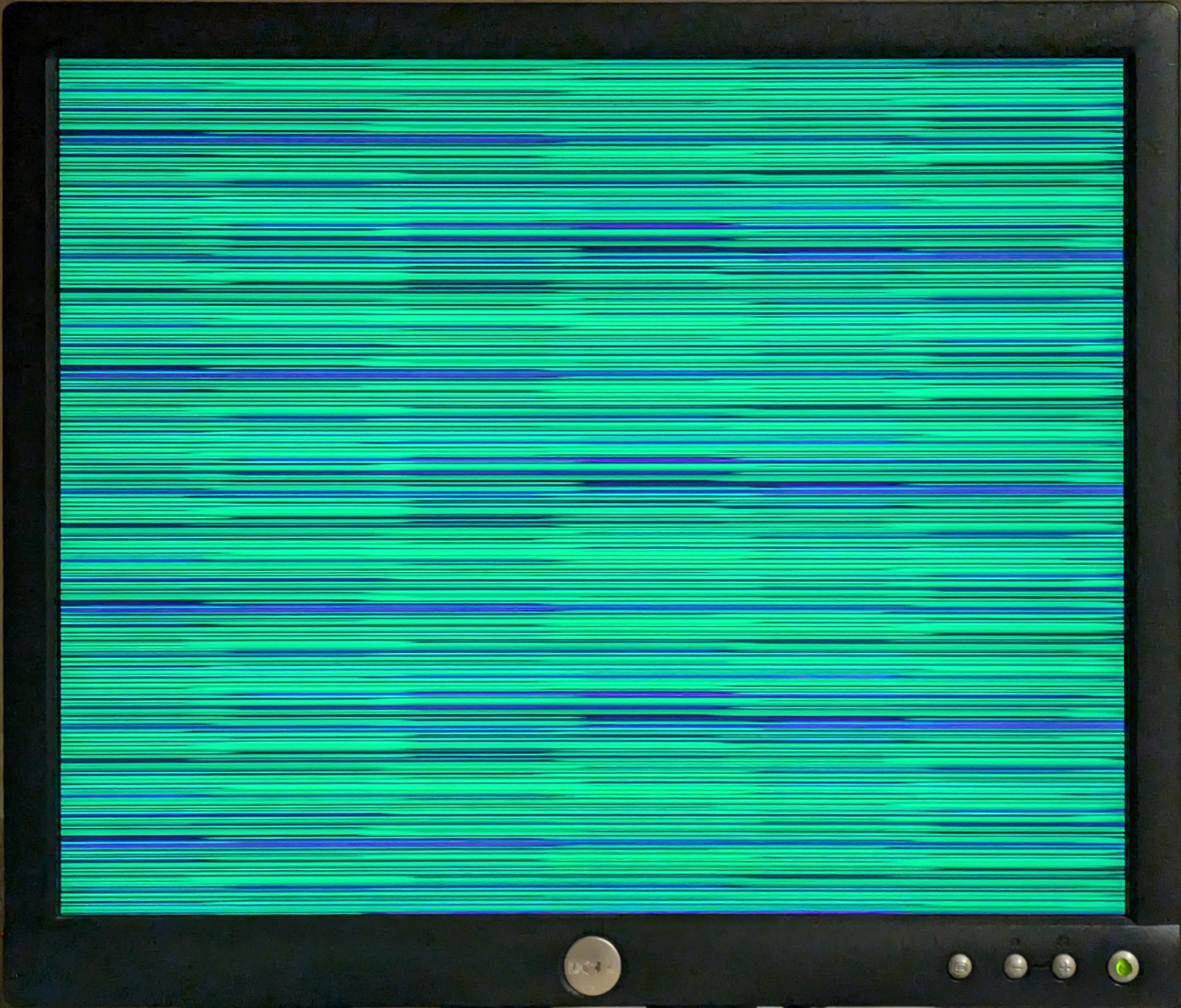
Now that wasn't looking very much like the data that I wanted to DMA into DAC. It was also changing quite a bit based on what exactly the code around it did (like adding something do a debugging ringbuffer). It appears that the DMA unit doesn't go through the CPU caches, so likely this was some random data.
After some digging I found out that there's different kinds of memory on this chip that are configured differently in Hubris.
You can see that configuration in chips/stm32h7/memory-large.toml.
Among others there's a dma flag that can be set for a region.
I'm not sure what that does exacly (it looks like one thing is that the kernel will refuse to copy
from or to there), but putting my buffer there using the link_section
attribute seems to make our DMA work.
After I got that to work all that was left was a lot of confusion because I had gotten the math for the pixel timing wrong. But after I had figured that out I was able to produce a nice gradient.
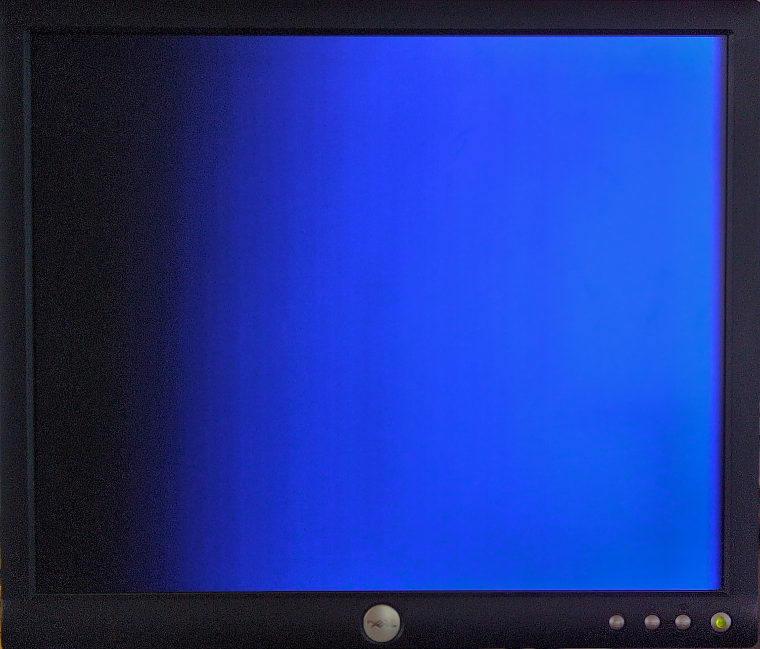
(If you're confused about the color: I had switched to blue instead of green at some point.)
Switching between on and off pixels leads to a pattern like this:
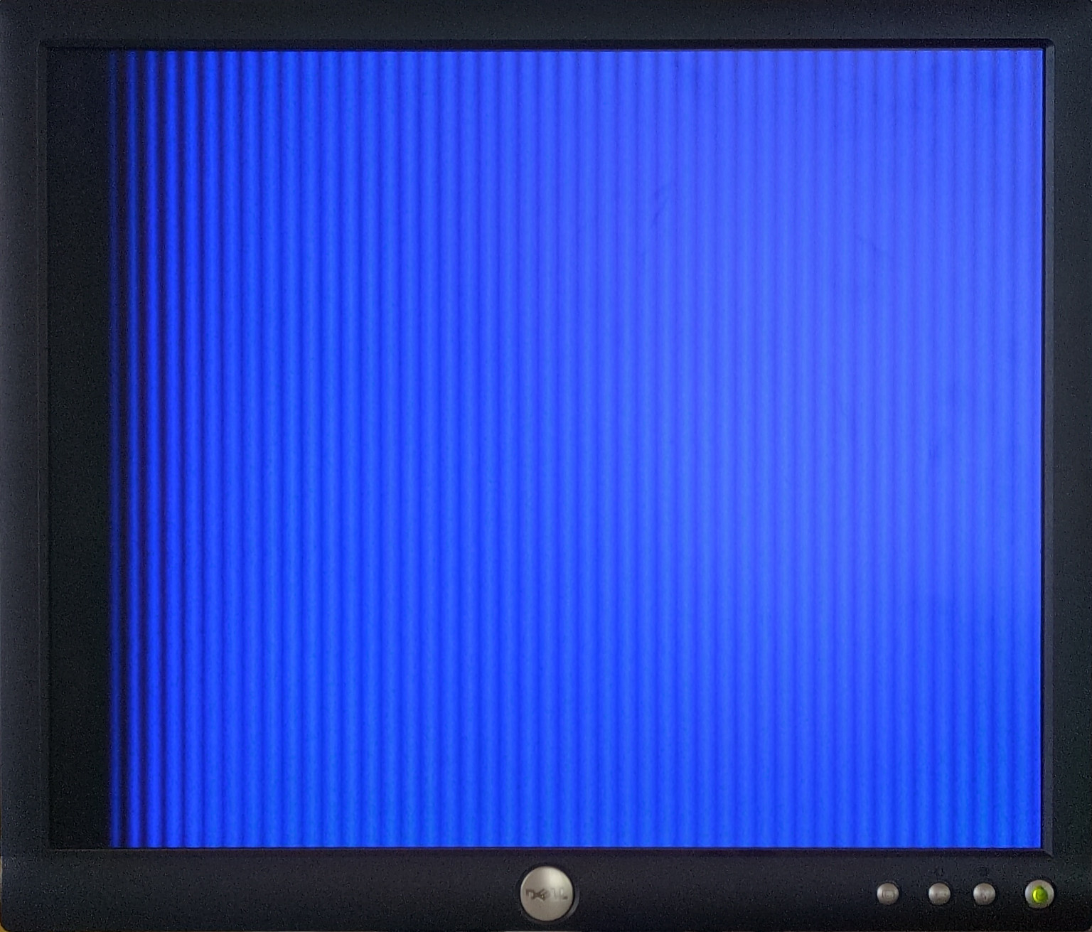
The DAC seems unable to produce sharp edges and also the average output seems to get higher after switching on and off a couple of times.
Here they used the SPI hardware support to produce an image, so maybe I should try that next as well.
Return of the Sys Task
The next thing I wanted to do of course was to produce an actual 2 dimensional image. So far the CPU hadn't been involved after setting up the registers. The DMA would keep going even if the CPU was halted.
This starts to become a problem for a 2D image though. If we were to keep our circular mode buffer and wanted to store a whole image in it we'd need a bunch of bytes for that. While we can horizontally repeat the same pixel 8 times (by decreasing the timer frequency), we can't do that vertically. So we'd need 132 (1056 / 8) × 628 = 82896 bytes for that buffer.
That would fit into one of the sram regions, but it's a bit of an inconvenient format for a framebuffer with vertical pixels being 8 times smaller than horizontal ones.
Luckily there's the master direct memory access controller (MDMA), which can be triggered by the completion of other DMA controllers and supports much more complex configuration.
But at this point I was definitely out of regions that could be mapped to my task.
Since it was very clear at this point that we weren't goint to do high speed GPIO toggling on the CPU we could actually re-introduce the sys task.
This means that we could get rid of two regions from our task (RCC and GPIO) and we'd have space for the MDMA control registers.
It's kind of funny how this hardware limitation can encourage splitting things into different tasks.
I was able to get the MDMA copying into the DMA buffer, but I haven't quite been able to get a framebuffer working yet. So this is the end of this post. I hope I'll find some more time for this project soon and I'll try to make another post if I get something more interesting going. I already have some ideas about what to do with a working framebuffer.